
OSP (Organic Solderability Preservative), which is a coating of organic copper trioxide (complex compound) grown on the surface of copper by chemical method. This organic coating can protect the clean bare copper on the circuit board from rusting (vulcanization or oxidation) in the normal storage environment, and can be easily soldered and dilute acid during the assembly of the pcba circuit board. Quickly remove and expose clean copper surface and weld with molten solder.
What are the features of OSP?
The OSP is basically a transparent protective film, which is usually very difficult to detect with the naked eye. Experts can see if there is a transparent film on the copper foil by refracting and reflecting light. And because the board that has done OSP and general bare copper sheet are not very different in appearance, this also causes the difficulty of the inspection and measurement of the product value of the plate factory. If OSP has a hole in the copper surface, the copper surface will be oxidized from the hole, which will affect the poor smt assembly, and the thicker the organic copper protectant, the better the protection of copper foil. However, relatively active flux is also needed to clear it for welding, so the thickness of OSP film is generally required between 0.2-0.5um.
The OSP is basically a transparent protective film, which is usually very difficult to detect with the naked eye. Experts can see if there is a transparent film on the copper foil by refracting and reflecting light. And because the board that has done OSP and general bare copper sheet are not very different in appearance, this also causes the difficulty of the inspection and measurement of the product value of the plate factory. If OSP has a hole in the copper surface, the copper surface will be oxidized from the hole, which will affect the poor smt assembly, and the thicker the organic copper protectant, the better the protection of copper foil. However, relatively active flux is also needed to clear it for welding, so the thickness of OSP film is generally required between 0.2-0.5um.
How about the Flow Chart of OSP Surface Treament?
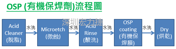
Acid cleaner (degreasing): the main purpose is to remove the pollution of copper oxide, fingerprint, grease and so on, so as to get clean copper surface.
Micro-etch (micro-etching): the main purpose of micro-etching is to remove the serious oxides on the copper surface, and to produce a uniform and bright micro-rough copper surface, so that the subsequent OSP film can grow more evenly and more evenly. There is a positive correlation between the luster and color of copper surface after OSP film formation and the selected micro-etching solution, because different potions can cause different roughness of copper surface.
Acid rinse (pickling): the function of pickling is to thoroughly remove the residue on the surface of copper after microetching to ensure that the surface is clean.
OSP coating (organic flux treatment): a layer of organic copper oxide film is formed on the copper surface to protect the copper surface from atmOSPheric contact and oxidation during storage. The thickness of OSP film is generally required between 0.2-0.5um.
The factors affecting OSP film formation are: ph value of OSP bath solution concentration of total acidity of OSP bath solution after operation temperature and reaction time OSP the washing of OSP bath solution should be strictly controlled over ph2.1. In order to avoid excessive acid washing, OSP skin film bite dissolution, resulting in a lack of thickness.
Dry (drying): in order to ensure that the coating layer in the plate and hole is dry, it is recommended to use 60-90 °C hot air blowing for 30 seconds. (this temperature and time may vary depending on the OSP material.)
What are the advantages of OSP?
1.low price.
2.Good welding strength.OSP copper base welding strength is basically better than enig nickel base.
3.Expired (3 or 6 months) board You can also do surface treatment again. But usually limited to one time, but also depends on the status of the board.
What are the disadvantages of OSP?
1.Hard to measure the thickness. (OSP is transparent thin film.)
2.Limited duration time. In general, as long as OSP is completed in the plate plant, the duration of the storage (shelf life) is up to six months, but some of them only last three months,depending on the capacity of the plate plant and the quality of the board.
3.Easily affected by acid and humidity. The shorter the time, the better the effect of one return welding and secondary return welding. It is generally recommended in 8 hours or 12 hours to back welding.
4. The test point must be printed with solder paste before electrical testing. (OSP is the insulating layer.)
5. Shorter and lower life circle. OSP board is a copper base. After soldering, it will generate a benign IMC of Cu6 Sn5, but after aging, it will gradually change to the inferior IMC of Cu3Sn, which has a bad effect for a long-term using.
How do we think of OSP?
In Shenzhen Grande's opinion, OSP surface treatmentcircuit board, the price of OSP is cheap, the solderability is good when fresh, the welding strength is good at the beginning, the weldability becomes worse after using for a period of time.
On one hand, Shenzhen Grande believes that OSP is very suitable for consumer products produced in a one-off mass production. It would be more perfect if the IMC generated by OSP and solder could be used for a period of time (after the warranty period) to change from benign Cu6Sn5 to strong Cu3Sn.
On the other hand,OSP is not suitable for a small variety of products, nor for products where demand estimates are not good for (demand forecast). If the company's PCB inventory is often over six months, it is really not recommended to use a OSP surfacing board. If not, it’s like "hit yourself in the foot with a brick", too silly.


