Vias-in-pad or vias-on-pad is a very headache for printed circuit board assembly factories, especially when the vias are placed on the BGA (Ball Grind Array) pad. However, design units often force assembly factories to follow suit due to insufficient design space or other insurmountable reasons.
As a matter of fact, with the shrinking of electronic products, the density of circuit boards is getting higher and higher, and the number of layers is increasing. Therefore, plenty of PCB layout engineers (CAD layout engagers) place the through holes on the solder pads; However, those small pitch BGA pads do not really have much space for the vias.
However, placing vias on the soldering pads saves space on the circuit board, but it is a catastrophe for SMT and manufacturing engineers, because it is likely to cause the following quality problems. Uncertainly, it was RD himself who returned to the carbine at the end:
1. If the via is placed on the solder pad of the BGA, it is likely to form a head-in-pillow (pillow effect or double-head effect) or bubbles inside the solder ball (Bubbles).
Because the solder paste is printed on the via hole, the air will be enclosed in the via hole. When the circuit board flows through the high temperature zone of the reflow furnace, the air in the via hole will expand due to heat and try to escape. The air that does not go out will form holes (Void/bubble) in the BGA solder balls, and in severe cases, it may even cause the head in pillow.
2. When the air accumulated in the through hole flows through the reflow oven, the air will be thermally expanded and there is a danger of out-gassing.
This usually occurs in a poorly preheated reflow profile. When the temperature rises too fast, the air expands rapidly, and the gas cannot escape effectively, and it will eventually burst out of the solder ball.
3. The solder paste will flow into the via hole due to pertaining to capillary, resulting in insufficient amount of tin that must be soldered in contact or lack of solder, etc. Or even flow to the opposite side of the board, causing a short circuit.
However, as product designs are getting smaller and smaller, PCB layout engineers have reached the point where they must compare the territory of the circuit board, and sometimes there should be room for compromise. Therefore, there are some alternative methods to deal with the through holes on the solder pads. The following figure shows five types of through holes from A to E and their impact on the SMT process:
Five designs of vias-in-pad

A) The vias are not processed at all.
This should not be accepted by manufacturing engineers, because tin will flow through this via hole after being heated, resulting in insufficient soldering, empty soldering and other undesirable phenomena, and the amount of tin is completely uncontrollable, and it may affect the parts on the other side of the board. Cause a short circuit.
C) Blind hole.
It can barely be used, but there is still a big risk. The amount of tin can be controlled, but when the solder paste covers the semi-buried hole, the air will be sealed in the semi-buried hole. When the circuit board passes through the reflow oven for heating, the air will explode the solder paste due to expansion, or form an escape channel. Short-term use may be no problem, but after long-term use, it may slowly crack from the escape channel, resulting in poor contact.
B) and D) are the best via design.
There are no holes on the solder paste pad to affect the amount of solder paste, and no additional bubbles are formed.
E) It can be used, but the price is much expensive.
A copper electroplating process can be added after the circuit board process to fill up the semi-buried holes or through-holes. The filled holes will be slightly sunken, so they must be controlled within a certain size, especially 0.5mm pitch BGA board. Note: The board of this process generally increases the price by about 10%.
In some BGA layout, in order to enhance the strength of the solder pad attached to the circuit board, the through hole is designed in the center of the BGA solder pad and the through hole is filled with copper, which is similar to punching a rivet on the solder pad to increase its strength.
The following is an example of the recently tamped QFN intermediate grounding pad. Nowadays, most of the QFN is used as a power controller, so its grounding and heat dissipation requirements are particularly high. The dense through holes like this can be used directly. The fate of solder paste printing is really strange results will happen.
↓This is the worst design. The through-holes are placed directly on the QFN grounding heat-dissipating pad, and the amount of tin cannot be ensured in manufacturing, and therefore, good soldering cannot be ensured.
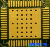
↓This is also a bad design, but some of the through holes have been covered with green solder mask, but there are still some through holes that are not plugged.
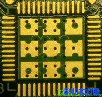
↓This design is barely acceptable, only a through hole in the middle is left without a plug hole, and the hole diameter is also reduced.
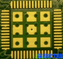
This is the worst through-hole design. The through-hole is placed directly on the QFN grounding heat-dissipating pad, and the amount of tin can not be ensured in manufacturing, and which also cannot ensure good soldering. This is also a bad through hole design, but some of the through holes have been covered with green solder mask, and there are still some through holes that are not plugged. The design of this through hole is barely acceptable, only the middle through hole is not plugged, and the hole diameter is also reduced.


