Analysis of Root Causes
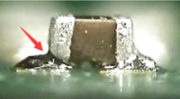
The root cause of the tombstone phenomenon is that the wetting properties (e.g., different wetting speeds) cause an imbalanced torque at the two ends of the chip terminals when the solder paste starts to melt. The tombstone phenomenon has other causes, including:
▪ The solder pads are improperly designed:
▪ The components’ terminals are not covered by more than 50% of PCB pads due to the space between the two pads is too wide.
▪ The two pads are designed with different sizes.
▪ The solder paste printing is uneven.
▪ The component placement is inaccurate.
▪ The reflow oven temperature is uneven.
▪ The thermal conductivity of the PCB material has different heating capacities.
▪ The presence of nitrogen has a tendency to increase the occurrence of the tombstone defect.
▪ Placing the chip parallel with the reflow oven’s conveyor.
Corrective Actions
▪ Design the pad sizes according to the recommendation specified on the datasheet.
▪ Reflow profile -- for lead-free solder paste, use a gradual soak ramp rate before reaching the melting point.
▪ Improve the accuracy of the solder paste printing.
▪ Impove the accuracy of chip placement by decreasing the placement speed.
▪ Esnure the pick and place nozzles have been adjusted to the correct pressure.
Another phenomenon is the OPEN circuit defect. This occurs when there is an electrical continuity OPEN circuit between at least one terminal of the chip and the solder pad. This phenomenon is very critical because even AOI cannot detect this failure most of the time.

Analysis of Root Causes
The root cause of the OPEN circuit phenomenon is similar to the tombstone defect. However additional causes must be considered:
▪ Component oxidization has occurred.▪ The pad sizes are not correct. The component’s terminals are not covered by more than 50% of PCB pads due to the space between the two pads is too wide.
▪ There is poor flux activity.
Corrective Action
▪ Design the pad sizes according to the recommendation specified on the datasheet.
▪ Select new components.
▪ Reflow profile -- for lead-free solder paste, use a gradual soak ramp rate before reaching the melting point.
▪ Adjust the pressure for pick and place nozzles.


