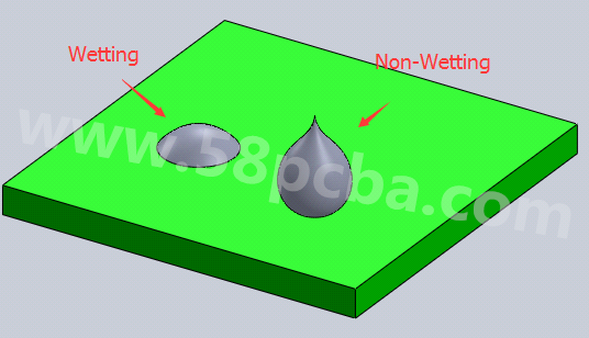
According to the IPC standard, non-wetting is defined as the inability of molten solder to form a metallic bond with the base metal. This results in the PCB pads or the component’s terminals not catching the solder during the reflow process.

Dewetting is a condition that results when molten solder coats a surface and then recedes leaving irregularly-shaped mounds of solder separated by areas covered with a thin film of solder and with the base metal. The surface finish is not exposed.
Dewetting usually refers to alloy solder joints that are not extended to PCB pads, so they do not obtain a good solder joint fillet. Dewetting directly impacts the quality of solder joints.
Root Cause Analysis
▪ The PCB pads or the component‘s pins are oxidized. An oxidation layer prevents contact between the solder and the surface plating layer.
▪ The plating thickness is too thin or the result of poor processing, which can be easily damaged during assembly;
▪ The soldering temperature is not high enough. Compared the SnPb solder , the melting point of lead-free solder alloy is higher and more difficult to wet.
▪ The preheat temperature is too low or the flux is inactive. The oxide layer on pads or the pin’s surface has not been removed effectively.
▪ The solder paste has expired, so its flux is inactive.
▪ There is a mismatch between the plating layer material and the applied solder paste.
▪ For 0201 and 01005 sized chips, since the amount of printed solder paste is thinner, the flux in the solder paste evaporates more quickly thus affecting the wetting properties of solder paste when using the same reflow profile.
▪ The solder paste or flux has been contaminated.
Corrective Action
▪ Pay close attention to the storage environment of PCB or the components. Ensure they meet the standards especially with regards to temperature and humidity.
▪ Select a PCB that has been certified to a plating thickness of more than 5μm.
▪ Don’t use a PCB that has been in storage for more than 1 year without any protective cover sheet.
▪ Don’t use expired solder paste.
▪ Select a reasonable reflow setup profile for a particular PCB.
▪ Solder wetting behavior can be significantly improved by using nitrogen in the reflow oven environment.
▪ For the 0201 and 01005 package components, decrease the pre-heat slope rate. Consider adjusting the stencil aperture size when printing.


