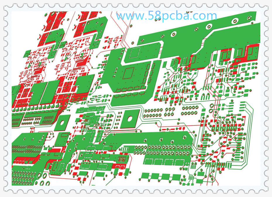
In fact, what we should do that is ensuring the components layout is reasonable and compact, and the routing channel is fully utilized, which is also the minimum difference between a veteran and a newbie.
For instance,
1.Avoiding through-hole circuit elements in your BOM wherever possible;
2.For SMT, using more 0603 components rather than 0805 or larger for power/RF passive components, and 0402 and maybe 0201 for others, such as bypass caps;
3.Finding the smallest packages, preferably fine-pitch or grid array, for the ICs and other semiconductors that you need;
4.Working with a board house that permits small trace widths, trace separation, and blind/buried vias if necessary;
5.Thicker copper can partially make up for thinner tracks and smaller polygon pours;
6.Increasing your layer count so that you don’t need that much wide fanout and branching to connect between the nodes at chip pads;
7.Break up your system into multiple sub-modules in separate circuit boards with connectors in between, which may even help keep your product enclosure size compact, at least in one or two dimensions, etc. [From Quora]


