Shenzhen Grande Electronic Linkedin Page
Shenzhen Grande Electronic Co., Ltd logo
E-mail us for a Quote:
sales88@greattong.com
Call us now:
+86-755-83261869

Technical Article


PCB Assembly: What is wave soldering?

Time:2017-04-14 10:37:27 Click:

PCB Assembly: What is Wave Soldering?
 

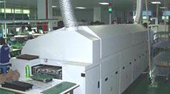
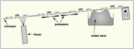
To solder a large number of electronic components on a Printed Circuit Board (PCB),  wave soldering is utilized. (That is to solder pins of components on a PCB.) Molten solder is held in a tank in which components are placed on the Printed Circuit Board. This stuffed PCB has to pass through a wave of molten solder or we can view it as a waterfall of solder.


Reliable electrical connections are developed when metallic areas on the PCB without solder mask (a solder resist coating on the surface of a PCB) are connected with solder once it is exposed to molten solder. A high quality product which is in fact better one done manually is quickly finished using this technique. 


This technique can be utilized for PCB Assembly SMT (Surface Mount) components as well as the through-hole ones.

Previous:PCB Assembly: Creating a Bill of Materials

Next:PCB Assembly:Design Decisions That Reduce Manufacturing Costs


Request an Official Quote

Questions

E-MAIL

File Upload

Upload a list of files

    Please upload your Gerber files and BOM. You can upload an unlimited number of files as long as the total size of all files does not exceed 20 MB. To ensure you receive your official quote in less than 24 hours, please include the quantity of circuit boards for which you would like a quote.

    If you require that we sign a Non-Disclosure Agreement (NDA), please send it to us prior to sending your files and we will be happy to accommodate.

     
    Home About Us Services Quality Pb-Free News Contact Us


    Copyright ® 2017,Shenzhen Grande Electronic Co., Ltd. All Rights Reserved. English 中文站 Sitemap