
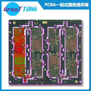
What is PCB copy board?
In a narrow sense, PCB copy board refers only to the process of extracting and restoring PCB files of electronic product boards and board cloning using files; In a broad sense, copy board not only includes board file extraction, board cloning, and circuit Board imitation and other technical processes, and including modification of the board file (ie, PCB modification), extraction and sorting of various electronic components on the electronic circuit board, decryption of the chip or micro controller encrypted on the circuit board, etc.
How about the implementation process of PCB copy board?
The technical realization process of PCB copy board is simply to scan the board to be copied, record the detailed component position, then remove the components to make a bill of materials (BOM) and arrange material procurement. Scanned into a picture and restored to a PCB board file by the copy board software, and then sent the PCB file to the plate making board. After the board is made, the purchased components are soldered to the finished PCB board, and then tested by the board. And debugging can be.
First of all, getting a PCB, then recording the model, parameters, and position of all the components on the paper, especially the direction of the diode, the three-stage tube, and the direction of the IC notch. It is best to take a photo of two positions at the digital camera with a digital camera. The current circuit board is getting higher and higher. The above diode triode is not noticed at all.
Secondly, all the multi-layer board parts are removed, and the tin in the PAD hole is removed. Clean the PCB with alcohol and put it into the scanner. When scanning, the scanner needs to slightly raise some scanned pixels to get a clearer image. Then polish the top and bottom layers slightly with water gauze, polish it to the copper film, put it into the scanner, start PHOTOSHOP, and scan the two layers in color. Note that the PCB must be placed horizontally and vertically in the scanner, otherwise the scanned image will not be used.
Thirdly, adjusting the contrast and brightness of the canvas so that the portion with the copper film and the portion without the copper film are strongly contrasted, then turn the secondary image to black and white to check whether the line is clear. If it is not clear, repeat this step. If it is clear, save the image as black and white BMP format files TOP.BMP and BOT.BMP. If you find any problems with the graphics, you can use PHOTOSHOP to fix and correct them.
Fourthly, converting the two BMP files into PROTEL format files, and transfer them into two layers in PROTEL. If the two layers of PAD and VIA are basically coincident, it indicates that the first few steps are very good. If there is a deviation, repeat the third step. Therefore, PCB copying is a very patient work, because a small problem will affect the quality and the degree of matching after copying.
Fifthly, converting the BMP of the TOP layer to TOP.PCB. Note that the layer to be converted to the SILK layer is the yellow layer. Then you trace the line in the TOP layer and place the device according to the drawing in the second step. Remove the SILK layer after painting. Repeatedly knowing to draw all the layers.
Sixthly, TOP.PCB and BOT.PCB are transferred in PROTEL, and it is OK to combine them into one figure.
Seventhly, the TOP LAYER and BOTTOM LAYER are printed on the transparencies (1:1 ratio) by laser printer, and the film is placed on the PCB. If there is any mistake, if you are correct, you are done.
A copy board like the original one was born, but it was only half done. Also test, test the electronic technology performance of the copy board is the same as the original board. If it is the same, it is really done.
Remark:
However, if it is a multi-layer board, carefully polish it to the inner layer, and repeat the steps of the third to fifth steps. Of course, the naming of the graphics is different. According to the number of layers, the general double-panel copy board is much simpler than a multi-layer board, and a multi-layer copy board is prone to misalignment, so the multi-layer board should be particularly concerned (internal vias and non-vias are prone to problems).


