In order to facilitate the clamping during the wave soldering of Printed Circuit Board Assembly ( PCBA ) , and avoid the collision of the components installed on the edge part with the clamping jaws, the adhesion between the edge wires and the clamping jaws, there should keep an area with no less than 5mm components area along the edge of the PCB as well as copper-free area are used as margin. As the picture shown below:
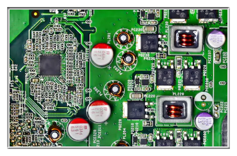
Since the PCB with array production, when the PCB that has been installed and soldered many times which will tend to be easy divided, the components lower than the edge area near the corner will inevitably endure greater torsion stress and deformation, which may cause additional stress and may cause solder joints and the components are cracked as a result. Compared with chip, SMD has no pins to eliminate the mechanical stress generated by PCB, so it is more likely to cause damage.
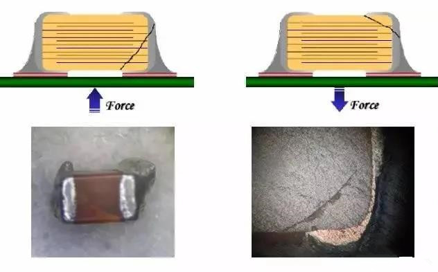
Therefore, the use of the pre-scribing line-joint structure can minimize the warpage and deformation during board splitting, and minimize the stress and defects on the components. The connection and separation of the jigsaw panels can be realized by the double-sided engraving V-Cut process. The depth of the V-Cut is "the sum of the double-sided depth is about 1/3 of the thickness of the board", which requires precise groove size and uniform depth. as the picture shown below:
PCBA Capability
1. The Largest Board: 310mm*410mm (SMT);
2. Maximum Board Thickness: 3mm;
3. Minimum Board Thickness: 0.5mm;
4. The Smallest Chip Package: 0201 package or parts above 0.6mm*0.3mm;
5. Maximum Weight of SMT Components: 150 grams;
6. Maximum Component Height: 25mm;
7. Maximum Component Size: 150mm*150mm;
8. Minimum Lead Component Spacing: 0.3mm;
9. The Smallest Ball Grid Array (BGA) Component Spacing: 0.3mm;
10. The Smallest Ball Grid Array (BGA) Component Diameter: 0.3mm;
11. Maximum Component SMT Accuracy (100QFP): 25um@IPC;
12. SMT Capacity: 3 to 4 million points/day.
Four Reasons Why Choosing Grande To Do PCBA
1. Strength Guarantee
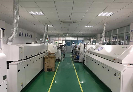
▪ SMT factory: With imported SMT machines and multiple optical inspection equipment, which is able to produce 4 million points per day. Each process is equipped with QC personnel who will keep an eye on product quality.
▪ DIP production line: Two wave soldering machines and more than 10 employees who have worked for over three years. That’ s to say, these workers are highly skilled and can weld various SMT & DIP components.
2. Quality Assurance With High Cost Performance
▪ High-end equipment can paste precision special-shaped parts, BGA, QFN, 0201 package. It can also be soldered prototype pcba via SMT machine and placing bulk materials by hand.
▪ Both samples, small and large batches can be produced. And there is no SMT Machine starting cost.
3. Rich Electronic Products SMT Soldering Experience With Stable Delivery
▪ Accumulated services to thousands of electronics companies, involving SMT soldering services for various types of automotive equipment and industrial control motherboards. Furthermore, PCBA products are often exported to Europe and the United States, and the quality is able to be affirmed by new and regular customers.
4. Strong Maintenance Ability & Reliable After-Sales Service
▪ The maintenance engineers have sophisticated experience so that those defective boards caused by all kinds of smt soldering can be repaired. Meanwhile, ensuring the connectivity rate of each circuit board also make sense.
▪Order problems feedback will get response, solution and solved as soon as possible.