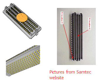
A high density SMT connector, such as the Samtec .050" SEARAY™ High Speed High Density Open Pin Field Array, has up to 500 I/O contact pins with a solder charge termination.

This type of connector looks like a standard BGA type of SMT device. A proper thermal profile for reflow must be evaluated by the process engineer prior to production.
▪ Thermocouple (TC) location
To verify the correct reflow profile, 2~3 thermocouples should be placed beneath the connector: one (1) in the leading corner position, one (1) in the middle of the connector, and one (1) at the trailing corner (optional). These theremocouple placements ensure that all areas of the connector receive even heating sumultaneously.
▪ Soak time and TAL consideration
To ensure proper temperature equalization of the whole area beneath the connector, it is recommended that the soak time is long enough as well as the time above liquidus be long enough for a total reflow. Of course, all data must meet with the solder paste manufacturer’s specifications.
▪ Preheat and cooling set point
A PCB’s physical properties are also another critical consideration for correct profile adjustment. In this case, the PCB has 16 layers and a 2mm thickness. This mean that this bare board has a high thermal resistance. So, the preheat set point can be adjusted higher than normal; however, the cooling point may lower than normal in order to meet TAL within the specifications.
Here are the testing results in this case study: (Note: this is for reference only):
▪ Reflow oven : Concept 7 zone
▪ TAL : 60 sec
▪ Peak temperature: 245°C
Board property
Zone 1
Zone 2
Zone 3
Zone 4
Zone 5
Zone 6
Zone 7
1.6mm, Dual layer, bare PCB
110
130
160
180
180
220
250
2.0mm, Dual layer, bare PCB
110
135
165
185
185
220
250
2.0mm, 16 layer, bare PCB
120
145
180
185
190
230
255
2.0mm, 16 layer, Samtec SEAM connector
125
150
185
195
195
255
275


