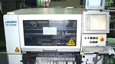
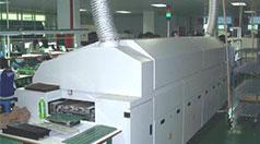
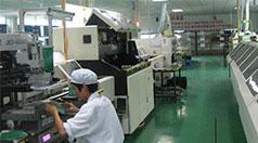
Shenzhen Grande Electronic functions with the help of latest technology, so our customers are not bothered about how does PCB x-ray inspection work and comfortably contact us for their various needs. We use advanced x-ray inspection tool to diagnose a variety of defects in PCB assembly components and for other processes.
We intend to deliver high-quality services with the support of experienced resources and advanced technology. We employ x-ray inspection for BGA, lead-less components such as QFN where the connections are not able to be seen and are beneath the IC. In this case, the normal optical inspection does not help to resolve issues. As the connections are below the IC package, it is important to make sure that the manufacturing procedures can hold these ICs accurately. X-ray inspection tends to give the desired results.
X-ray inspection tool exhibit grayscale drawing, which show variations in the form and thickness of a part. High-density features create a darker picture as compared to lesser density or thickness. As a result, it enables to quantitatively calculate these features and form association between suitable or unwanted manufacturing methods. Our qualified team uses x-ray inspection to resolve the majority of the problems. X-ray inspection is done in real time to continuously verify the quality steps followed. It assists us to examine the solder joints which are difficult to check via conventional methods. It also supports in validating oven profile.
X-ray inspection also allows us to authenticate oven profile. X-ray inspection identifies inadequate solder and moreover reveals the paste dispense process as the cause of a difficulty. Furthermore, automated x-ray system gathers measurement details of every joint and provides instant response to the performance of the assembly process.
X-ray inspection aids to disclose multiple defects i.e. whether unseen or evident, including short or open solder joints, lifted pins, part mis-registration, etc. X-ray technology is not only used to identify bad solder joints but even point to the area in the course that created the defect.
If there is any confusion regarding X-ray inspection process, kindly let us know, we will readily explain the complete process.
Welcome to Shenzhen Grande Electronic Co., Ltd.!


