
What is the resin plugging technology?
The process of resin plugging has been widely used in the PCB industry in recent years, especially in some products with high layer and large plate thickness. It is desirable to use resin plugging to solve a series of problems that cannot be solved by using green oil plugging or pressure-filling resins. However, due to the nature of the resin, it is necessary to overcome many difficulties in the production to obtain a good quality of the resin plugging product.
What is the origin of the resin plugging?
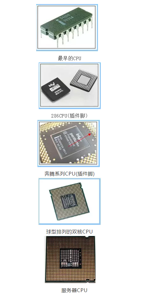
Development of electronic chips
With the continuous updating of electronic product technology, the structure and installation of electronic chips are constantly improving and changing. Its development has basically evolved from a component with a plug-in foot to a highly dense integrated circuit module which uses a ball matrix to arrange solder joints. The development history of components can be seen from the following figure:
The encounter between two people made the resin plugging technology
In the PCB industry, many process methods have been widely used in the industry, and people have basically not paid much attention to the origin of some process methods. In fact, when the electronic chip arranged in the spherical matrix was just launched, people have been making suggestions for such small chip-mounting components, and it is expected to reduce the size of the finished product from the structure.
In the 1990s, a Japanese company developed a resin that directly plugged the holes and then plated copper on the surface, which is mainly to solve the problem of air blowing in the green oil plug holes. Intel applied this process to Intel's electronics to create the so-called POFV (partially called Via on pad) process.


