Shenzhen Grande Electronic Linkedin Page
Shenzhen Grande Electronic Co., Ltd logo
E-mail us for a Quote:
sales88@greattong.com
Call us now:
+86-755-83261869

Technical Article


PCB Layout: High Voltage PCB Design Tips

Time:2017-05-15 15:53:08 Click:

Guidelines 
When drawing a PCB layout, it is very important to provide suitable clearance between traces and provide enough space between the components, especially in high voltage applications, in order to avoid any electrical arcing and breakdowns. 

Before designing the circuit, the designer should become familiar with the following technical terminology:
1. Functional insulation -- the insulation only required for circuit operation. It does not imply safety protection.
2. Basic insulation
3. Supplementary insulation
4. Double insulation
5. Reinforced insulation
6. Clearance
7. Creepage distance
8. Altitude
The grade of insulation, PCB type, environment and altitude will affect the clearance and creepage 

Distance 
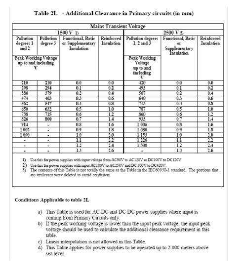
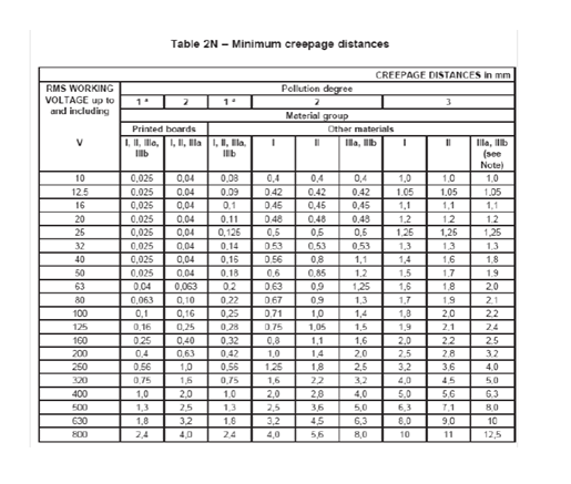
The PCB designer should follow safety standards such as UL60950-1(USA) or CSA 22.3 (Canada) minimum clearancesadditional clearanceminimum creepage
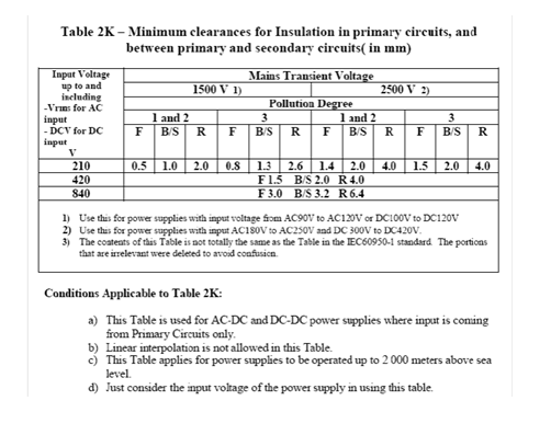
minimum clearances
additional clearance
minimum creepage

Previous:PCB Fabrication: Heavy Copper PCB

Next:PCB Fabrication: How Conformal Coating Protects PCBs


Request an Official Quote

Questions

E-MAIL

File Upload

Upload a list of files

    Please upload your Gerber files and BOM. You can upload an unlimited number of files as long as the total size of all files does not exceed 20 MB. To ensure you receive your official quote in less than 24 hours, please include the quantity of circuit boards for which you would like a quote.

    If you require that we sign a Non-Disclosure Agreement (NDA), please send it to us prior to sending your files and we will be happy to accommodate.

     
    Home About Us Services Quality Pb-Free News Contact Us


    Copyright ® 2017,Shenzhen Grande Electronic Co., Ltd. All Rights Reserved. English 中文站 Sitemap