Multilayer PCBs are widely used in the fields of communication, medical, industrial control, security, automobile, electric power, aviation, military, and computer peripherals. The more the corresponding number of layers, the higher the cost of multi-layer PCB Prototyp. So what are the difficulties in making multilayer circuit boards?

1. Difficulties in making inner circuit
Multi-layer PCBs have various special requirements, such as high speed, thick copper, high frequency, and high Tg values, which all cause the requirements in inner layer layout and pattern size control getting higher and higher. For example, the ARM development board, there are plenty of impedance signal lines in the inner layer. And in order to ensure the integrity of the impedance which are definitely going to increase the difficulty of producing the inner layer circuits.
Furthermore, if there are a lot inner layer signal lines, whose width and spacing of the lines are basically about 4mil or less; The production of multi-core and thin-layer boards is easy to wrinkle, and these factors will obviously increase the production of the inner layer.

Advice:Design the line width and line spacing above 3.5 / 3.5mil (In this case, there will be no difficulty for most PCB factories in production).
For example, six-layer board, it is recommended to use a similar eight-layer structure design, which can meet the requirements of line width 4-6mil and impedance 50ohm, 90ohm, 100ohm.
2. Difficulties in alignment requirement between inner layers
As the number of board layers increases, the alignment requirements of the inner layer are also getting higher and higher. The film will expand and contract under the influence of the temperature and humidity of the workshop environmen as well as the board, which makes the alignment accuracy between the inner layers more difficult to control.
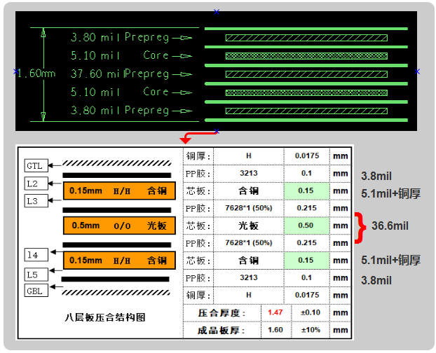
3. Difficulties in lamination process
The stacking of multiple boards and PP is prone to problems such as delamination, skateboard and drum residue during lamination. Therefore, in the structure design process of the inner layer, factors such as the dielectric thickness between layers, flow of glue and heat resistance of the plate should be considered, then designing the corresponding laminated structure reasonably.
Advice: keep the inner layer copper evenly, and balance copper in the same area without PAD.
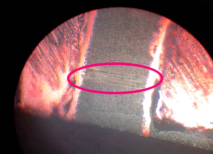
4. Difficulties in drilling production
Multi-layer boards use high Tg or other special plates. The roughness of the drilled holes of different materials is various, which increases the difficulty of removing rubber residue in the holes. High-density multi-layer boards have high hole density, low production efficiency, and easy to break the blade of drilling machine. That’s to say, if the hole edges of different networks are too close, the CAF effect will be caused. (CAF:Conductive Anodic Filamentation )
Advice: The hole edge spacing of different networks should be ≥0.3mm.