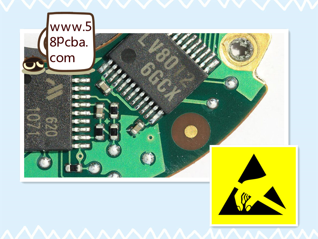
For instance,
1. Penetrating the thin insulating layer of components inside;
2. Damaging the grid electrode of the MOSFET and CMOS components;
3. The flip-flop is deadlocked in the CMOS components and the PN junction is short-circuited and reverse-biased;
4. Short-circuited and forward-biased PN junction; The soldering wire or aluminum wire inside the active device is melted.
In a word, electrostatic damage to the device is divided into visible and invisible damages. The invisible damage can not be observed at the time, but the com ponenet will become more fragile and easily be damaged under conditions of overpressure and high temperature.
PS: Electrostatic protection is usually designed from such three aspects: Preventing external charges from flowing into the board and causing damage; preventing external magnetic fields from damaging the board and preventing electrostatic fields from harming.


