Shenzhen Grande Electronic Linkedin Page
Shenzhen Grande Electronic Co., Ltd logo
E-mail us for a Quote:
sales88@greattong.com
Call us now:
+86-755-83261869

Technical Article


When creating a PCB, what is the difference between layout and artwork?

Time:2019-07-15 18:54:33 Click:

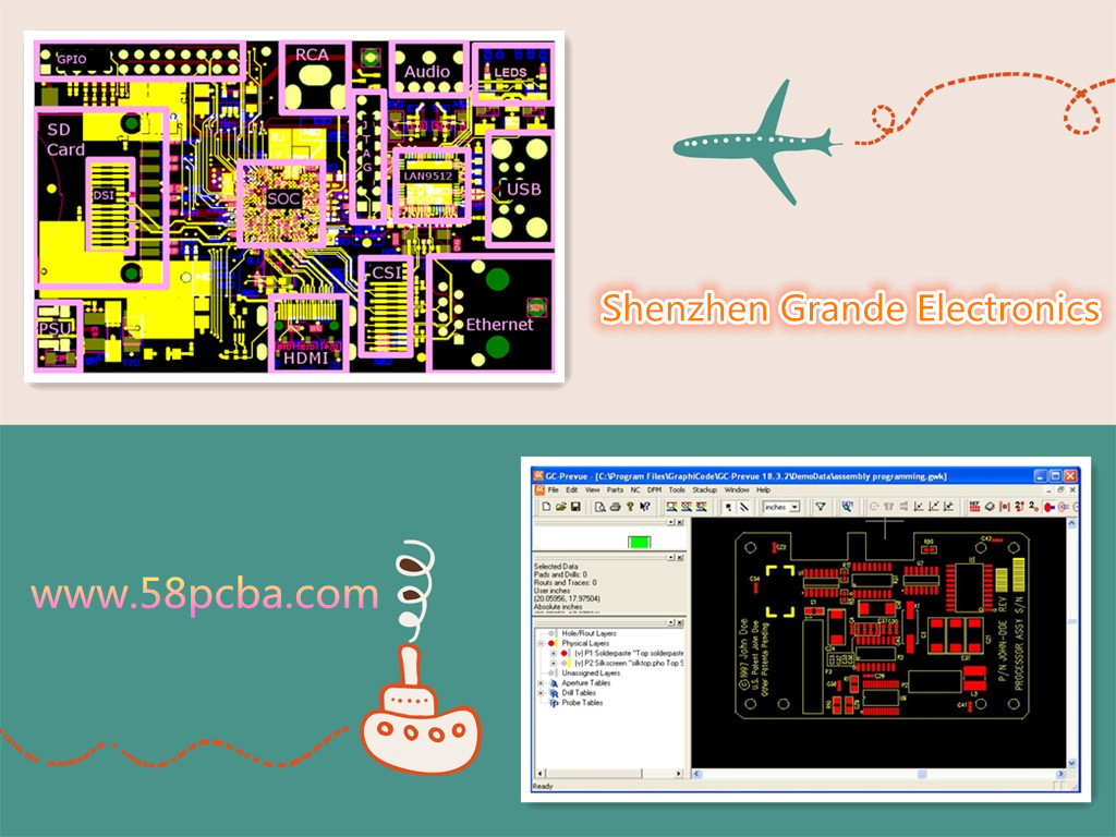
PCB layout is a broad term to refer to the many processes involved in designing a PCB, typically using EDA - Electronics Design Automation - CAD software; In addition, Layout is the design of overall arrangement, such as layout, routing.


After the PCB file design is completed, the graphic data is required for the PCB fabrication, that is the Artwork. That’s to say, Artwork can be considered as the Gerber that we usually say.


Previous:How do I start PCB designing?

Next:What equipment is used by professional PCB manufacturers?


Request an Official Quote

Questions

E-MAIL

File Upload

Upload a list of files

    Please upload your Gerber files and BOM. You can upload an unlimited number of files as long as the total size of all files does not exceed 20 MB. To ensure you receive your official quote in less than 24 hours, please include the quantity of circuit boards for which you would like a quote.

    If you require that we sign a Non-Disclosure Agreement (NDA), please send it to us prior to sending your files and we will be happy to accommodate.

     
    Home About Us Services Quality Pb-Free News Contact Us


    Copyright ® 2017,Shenzhen Grande Electronic Co., Ltd. All Rights Reserved. English 中文站 Sitemap