Supplier: Shenzhen Grande Electronic
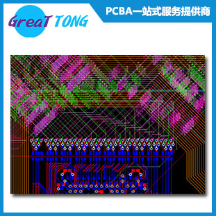
Layers: 6
Application: 6 Layers Module PCB Design PCB layout-PCB Manufacturer Shenzhen Grande
Software: PADS
Features: Matched length for data, address and clock’s traces, used different groups and layers
Design time: 5 Days
【Description】
PCB layout Features:
1, Matched length for data, address and clock traces.
2, Used different groups and layers
PCB Fabrication:
Layers: 6
Surface Treatment: Im Au
Material: FR-4/HTg170, 1.6mm, 1oz finished Copper
Impedance Control Tolerance: +/-10%
Others: 5/5mil,Via:8mil


