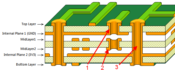
It seems that you are talking about trace layers of PCB. In fact, it includes both surface layer and inner layer, which are conductive by vias or pins of DIP components.
What’s more, these layers are generally called signal layer, power plane and ground plane.
