Why does the PCB need rinse after assembly?
The PCB need rinse after soldering at very first. That's to say, when the PCB has finished "Wave soldering" or "Surface Mount", The pollutants on the board will be cleaned with detergent or pure water. Gradually, as the design of electronic parts become more and more diverse and smaller. The rinsing process finally explores some problems. What's more, due to the PCB rinsing process is troublesome, as a result, no-washed PCB method shows up and caters for the market nowadays.
What is the purpose of rinsing?
Washing the board is to remove the flux remaining on the surface of the PCB.
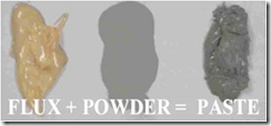
During the SMT process, the biggest difference between the "water-wash process" and the "no-wash process" is that the difference lies in the flux composition of the solder paste. The wave soldering process is purely a component of the flux before the furnace. This is because the main purpose of flux is that removing the surface tension and oxide of the object so as to be welded with a clean soldering surface. The best chemical medicine for removing oxidation is chemical "acid" and "salt", but they are corrosive. If it remains on the surface of the PCB, it will corrode the copper surface and cause serious quality defects future.
In fact, even if the PCB is produced with using a no-wash process, as long as the flux is not properly formulated (usually some unknown solder pastes or the solder paste with special emphasis on tin or oxide were used.) Since these solder paste fluxes usually add weak acid or much flux residue. Therefore, the solder paste may corrode the copper surface of the board after mixing with moisture and pollutants in the air for a long time. Cleaning is necessary when the board is at risk of corrosion. In other words, the "no-wash process" board may also need to be rinsed.
What are the benefits of rinsing?
▪ To leave a good impression to the customer.
▪ To increase the surface adhesion of the board in the subsequent process of PCBA. For example, Conformal coating need to pass the Cross-Cut Test.
▪ To avoid unnecessary chemical reactions in solder paste residues, such as the Potting process.
▪ To avoid leakage current or increase the retention current.
If the flux is still remaining the PCB, it will lead to the problem of micro-conduction (lower impedance) in humid environments, especially for those fine-pitch parts, such as the bottom of passive components below 0201 and narrow spaces BGA package( the pads is placed at the bottom of the part, which is easy to remain much flux. Furthermore, the moisture is also easy to be attached to the underside when it is not used. Then it will form micro-conduction for a long time.


