The benefits of embedded PCB components is still a relatively new process, yet fabrication houses around the world are turning to this manufacturing process to eliminate problems such as parasitic effects and to reduce the PCB footprint, both of which are critical to the growth market of mobile technology products.
New developments in PCB fabrication methodology, supported by improvements in electronic design automation solutions, have brought PCB component embedding processes to the marketplace at a time when PCB complexity has escalated resulting in designs with greater density resulting from the evolution of mobile product technologies in recent years.
Essential Benefits
Improved PCB performance in a smaller footprint is the most touted benefit of embedding components in the PCB substrate. But the benefit of embedding is not a one-size-fits-all approach. Electronic design engineers must make choices of whether to use embedding or not, and if used, under what conditions.
As previously stated, the recent innovations in PCB technology have been driven in large part by increases in not only processing power, but also component integration, which in turn have driven smaller PCB footprints, resulting in lower production costs. Embedding PCB passive components is part of this component integration trend. Moreover, when considering the cost of complex, multi-layer PCBs, embedding becomes an ever more attractive choice in the universal quest of maintaining product costs as low as possible in a globally competitive world.
But costs alone should not be the primary decision point on whether to use PCB component embedding or not. Think of it this way: in terms of performance, can component embedding offer benefits that would otherwise not be possible? The answer is a resounding yes!
Eliminating Parasitic Effects
Parasitic capacitance and inductance in high frequency circuits can cause undesirable noise as wells as fluctuating loads if the wire lengths between ICs are too long. To reduce or eliminate parasitic effects has been challenging. But PCB component embedding offers a reliable way to eliminate the problems associated with these parasitic disturbances. By positioning passive PCB components beneath IC pins can reduce vias inductance and minimize the adverse effects of parasitic disturbances. Only by embedding PCB components can this benefit be realized at an acceptable cost.
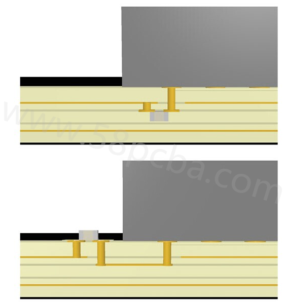
Noise that is capacitively- or inductively-coupled can be reduced by placing an EMI shield around an embedded integrated circuit. This can be done by placing through-holes that are plated around the IC. In some applications, this benefit can take away the requirement of having another surface-mounted shield.
Thermal Management Benefits
Embedding can also take on the additional function of thermal management. Embedding components can be modified with heat conductive features that solve thermal problems. For example, heat can be dissipated in a thermal layer by embedding thermal micro-vias so they are in physical contact with the embedded component. This approach will reduce thermal resistance since it limits the distance that the heat will need to travel across the PCB substrate.
Reliability
One of the challenges of embedding components is the concern for extended reliability since these components cannot be tested or replaced easily if a PCB fault occurs. Reliability should always be considered when deciding on incorporating component embedding into a PCB design. An electronic design engineer should consider the reliability of solder joints in the laminate framework, as well as any other soldering processes, especially reflow soldering of SMDs.


