
1. The spacing between SMT components
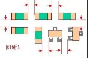
The spacing between SMD components is an issue that engineers must pay attention to when designing PCB. Because if the pitch is too small, then it will be quite difficult to print solder paste and avoid solder joints.
The recommended distance is as follows:
Equipment distance requirements between SMT components:
Similar equipment: ≥0.3mm
Heterogeneous equipment: ≥0.13 * H + 0.3mm (H is the maximum height difference between adjacent components)
The distance between the components that can only be pasted manually: ≥1.5mm
The above suggestions are for reference only and can be consistent with the PCB process design specifications of the related companies;
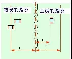
2. Directly insert the distance between the device and the chip
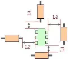
As shown in the figure above, a sufficient distance should be maintained between the direct insertion resistance device and the chip. It is recommended to be between 1-3mm. Due to processing difficulties, direct plugins are rarely used now.
3. Decoupling capacitors used to place the IC
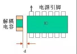
Decoupling capacitors should be placed near each IC power port and should be placed as close as possible to the IC power port. When a chip has multiple power ports, a decoupling capacitor should be placed on each port.
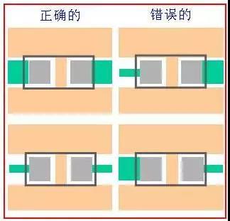
4. Pay attention to the placement direction and distance of components on the edge of the PCB
Generally, PCBs are made of panels, so devices near the edges need to meet two conditions.
The first one is parallel to the cutting direction (for example, if the device is placed on the left side of the figure above to make the mechanical stress of the device even, when the panel is split, the two pads of the SMT patch are different, which may cause Components and pads dropped)
The second problem is that the equipment cannot be arranged within a certain distance (to prevent damage to the components when cutting the circuit board)
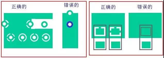
5. Pay attention to the conditions that need to connect adjacent pads
If you need to connect adjacent pads, please make sure to connect them to the outside first to prevent them from being connected in groups. At this time, please pay attention to the width of the copper wire.
6. If the gasket falls in a public area, heat dissipation should be considered
If the mat falls in the paved area, the correct method should be used to connect the mat to the paved area. In addition, according to the current size, determine whether to connect 1 wire or 4 wire.
If the left method is used, it is difficult to weld or repair and disassemble, because the temperature will be completely dispersed due to the copper coating, resulting in poor welding.
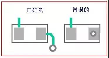
7. If the wire is smaller than the insertion pad, you need to add some teardrops
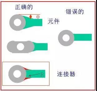
If the wire is smaller than the pad of the embedded device, please add a teardrop on the right side of the picture above.
Increasing tears has the following benefits:
(1) In order to avoid reflections caused by a sudden decrease in signal line width, the connection between the wiring and the component pad tends to be smooth.
(2) The problem that the connection between the pad and the wire is easily broken under impact is solved.
(3) Setting water droplets can also make the PCB more beautiful.
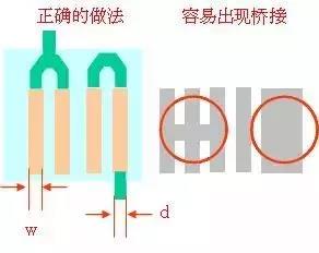
8. The lead width on both sides of the component pad should be the same
9. Be careful to keep the mat pin-free and grounded
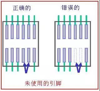
For example, if two pins of the chip in the picture above are not used, but there are physical pins of the chip, if two pins are suspended in the way on the right side of the picture above, it is easy to cause interference. Also, if the pad is added and the pad is grounded, interference can be avoided.
10. It is best not to make through holes on the pads
It is best not to punch through holes in the pads, otherwise it will easily cause solder leakage.
11. Pay attention to the distance between the conductor or component and the edge of the board

Please note that wires or components should not be too close to the edge of the board, especially a single panel. Usually, a single panel is mainly cardboard, which is easy to break when subjected to pressure. If you connect wires or place components on the edge, they will be affected.
12. The environment temperature of the electrolytic capacitor must be far away from the heat source
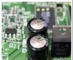
First of all, the environment temperature of the electrolytic capacitor should be considered to meet the requirements. Second, the capacitor should be as far away from the heating area as possible to prevent the liquid electrolyte inside the electrolytic capacitor from drying out.


