Solder bridging occurs randomly between LED pads. It is pretty hard to detect because it could be happening underneath the components. Only a functional test can tell you what’s wrong with the light color emitting LED.
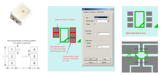
When we checked the LED pads on a bare PCB with a microscope, we observed there there was no solder mask in the gap between the pads. Furthermore, after we reviewed the pads’ design in EDA software and found that the size of the pad’s solder mask override was 0.106mm (4 mil) as the default value. But the gap between the pads was only 0.2mm as per the PCBA manufacturer’s recommendation. It was less than twice the solder mask override (2 x 0.106 = 0.212mm). This confirmed that there was no solder mask between the pads. When we placed the LED onto the board, the solder paste on the pads was squeezed to the edge of the pads. It was possible for them to be in contact with one another because the gap was small. We think this was root cause of the defect.
The next step was to redesign the pads’ solder mask size. We set up manually the solder mask override value to 0.
We also redesigned a new stencil for paste printing with a shrinking aperture size width from 0.65mm to 0.55mm and an extending aperture size length from 0.85 to 0.95 mm.
The production results were very positive. The solder bridging defects dropped down to zero in the following 10,000 pcs assembly.
* 3528 (body size 3.5 x 2.8 mm) PLCC (6-pin package) RGB LED


