
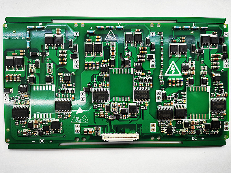
Grande Electronics is also a PCB Design company, specializing in electronic product circuit board layout. It mainly runs multi-layer, high-density PCB layout and PCB layout prototype. Now, I will introduce the layout principles of PCBA control board.
Components Layout Precautions for PCBA Control Board
1. When it comes to the layout of PCB components, components related to each other should be placed as close as possible. For instance, clock generators, crystal oscillators and CPU clock input terminals are prone to noise. When placed, these mentioned components should be placed close to each other. However, regarding those components that are prone to noise, low-current circuits, high-current circuit switching circuits, etc., keep them away from the microcontroller logic control circuit and storage circuits (ROM, RAM) as much as possible. If possible, these circuits can be made into circuit boards, which is beneficial anti-interference, improve the reliability of circuit work.
2. Try to install decoupling capacitors next to key components such as ROM and RAM chips. In fact, PCB layout, pin layout may contain large inductive effects. Large inductance may cause severe switching noise spikes in the Vcc layout. The only way to prevent switching noise spikes in the Vcc layout is to place a 0.1uF electronic decoupling capacitor between Vcc and the source. If a surface mount component is used on the circuit board, the chip capacitor can be placed directly against the component and connected to the Vcc pin. It is best to use ceramic tile capacitors because of their low ESL electrostatic loss, high frequency impedance, and good dielectric stability over temperature and time. Since tantalum capacitors have high impedance at high frequencies, tantalum capacitors should not be used as much as possible.
Pay attention to the following points when placing decoupling capacitors on PCB layout of PCBA control board:
1. The power input terminal of the printed circuit board is connected to an electrolytic capacitor of about 100uF. If the volume allows, a larger capacity will be better.
2. In principle, a 0.01uF ceramic capacitor should be placed next to each IC chip. If the gap of the circuit board replica is too small to be placed, 1-10 tantalum capacitors can be placed for every 10 chips.
3. A decoupling capacitor should be connected between the power line (Vcc) and the ground line to deal with components with weak anti-interference ability and large current changes during shutdown, as well as storage components such as RAM and ROM.
4. The capacitor lead should not be too long, especially for high-frequency bypass capacitors.
In the single-chip control system, there are many kinds of ground wires, such as system ground, shield ground, logic, simulation ground, etc. Whether the PCB layout of the ground wire is reasonable or not which will determine the anti-interference ability of the circuit board. At the time of layout the ground wire and connection of the PCBA control board, the following precautions should be considered:
1. Logic and analog grounding should layout separately and cannot be used together. Connect their respective ground wires to the corresponding power ground wires. In PCB Layout, the analog ground wire should be as thick as possible, and the ground area of the front end should be increased as much as possible. Generally speaking, for input and output analog signals, MCU circuits are best separated by optocouplers.
2. When layout the printed circuit board of the logic circuit, the grounding wire should form a closed loop to improve the anti-interference ability of the circuit.
3. The ground wire should be as thick as possible. If the grounding wire is very thin, the resistance of the grounding wire will be very large, causing the ground potential to change with the change of current, resulting in unstable signal level, thereby reducing the anti-interference ability of the circuit. If the wiring space permits, ensure that the width of the main ground wire is at least 2~3mm, and the ground wire on the component pins should be about 1.5mm.
4. Pay attention to the choice of venue. When the signal frequency on the circuit board is lower than 1MHz, the electromagnetic induction between layout and the components has little effect, and the circulating current formed by the grounding circuit has a greater influence on the interference, so the grounding point should be used. Avoid forming a loop. When the signal frequency on the circuit board is higher than 10MHz, the ground line impedance becomes very large due to the obvious inductive effect of the wiring, so the circulating current formed by the ground circuit is no longer a major problem. Therefore, multi-point grounding should be used to minimize ground impedance.
5. In addition to making the power line width of PCB layout as thick as possible according to the size of the current, the power line and the direction of the ground line should be the same as the data line of the square wiring. When the layout work is completed, the ground line will connect the circuit board The bottom of the circuit is not covered, these methods can help enhance the anti-interference ability of the circuit.
6. The width of the data line should be as wide as possible to reduce impedance.
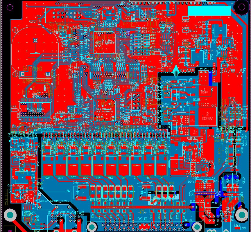
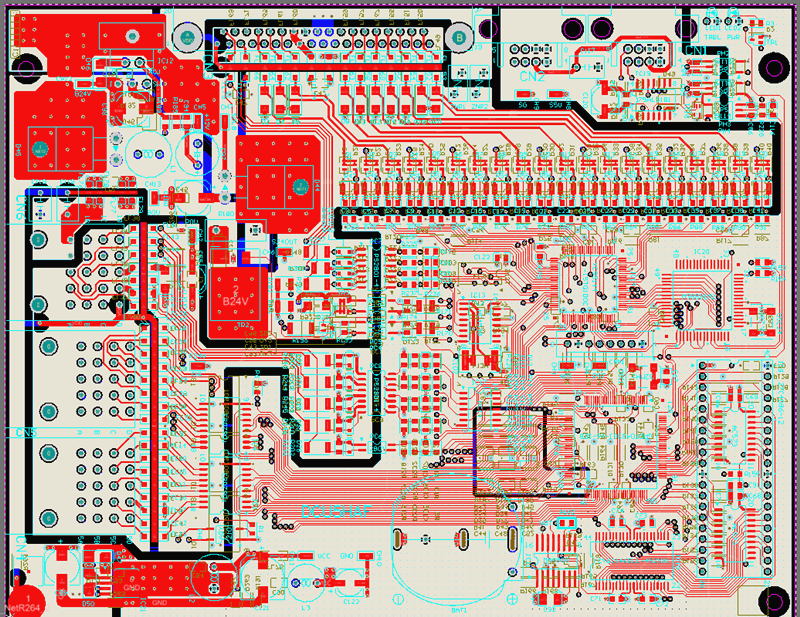
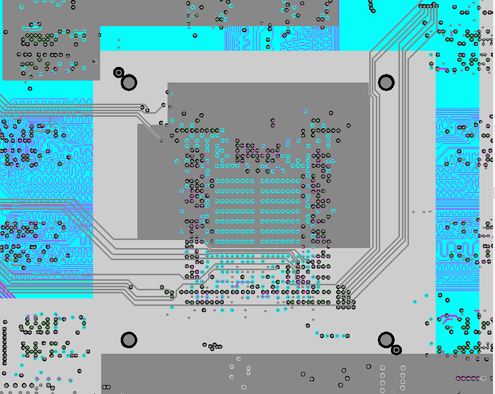
Grande Electronics PCB Layout Ability:
The Highest Signal Layout Rate: 10Gbps CML differential signal;
The Highest PCB layout Layers: 40 layers;
Minimum Line Width: 2.4mil;
Minimum Line Spacing: 2.4mil;
Minimum BGA PIN Spacing: 0.4mm;
Minimum Mechanical Via diameter: 6mil;
Minimum Laser Drilling Diameter: 4mil;
Maximum PIN Number:; 63000+
Maximum Number Of Ccomponents: 3600;
Maximum Number Of BGA: 48+.


