Shenzhen Grande Electronic Linkedin Page
Shenzhen Grande Electronic Co., Ltd logo
E-mail us for a Quote:
sales88@greattong.com
Call us now:
+86-755-83261869

Technical Article


Why are vias bad for high-frequency PCBs (Printed Circuit Boards)?

Time:2018-11-09 09:34:40 Click:

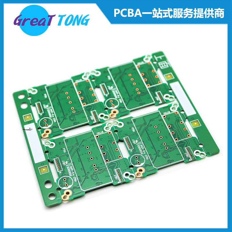
Via is made of drill hole +pad area around the drill hole.


During the high speed and high frequency PCBs, a lot vias are obviously bad.


1)Via will take up a lot spaces, which is bad for PCB Layout.

2)Via as the breakpoint of the impedance discontinuity in transmission line, which will cause a reflection of a signal.


Previous:How do I Become a PCB Design Trainer?

Next:What is a "buried via" on an electronics PCB?


Request an Official Quote

Questions

E-MAIL

File Upload

Upload a list of files

    Please upload your Gerber files and BOM. You can upload an unlimited number of files as long as the total size of all files does not exceed 20 MB. To ensure you receive your official quote in less than 24 hours, please include the quantity of circuit boards for which you would like a quote.

    If you require that we sign a Non-Disclosure Agreement (NDA), please send it to us prior to sending your files and we will be happy to accommodate.

     
    Home About Us Services Quality Pb-Free News Contact Us


    Copyright ® 2017,Shenzhen Grande Electronic Co., Ltd. All Rights Reserved. English 中文站 Sitemap