
If you want to solve the problem of BGA Solder cracking thoroughly, you have to understand "where does the stress come from?"
How many types of Stress?
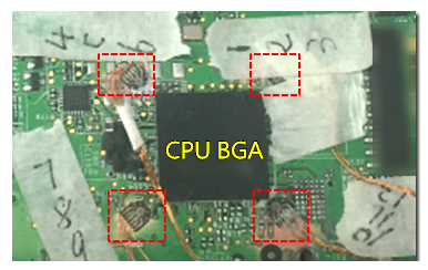
Stress can be divided into internal stress and external stress. Internal stress belongs to the long-term reliability of latent (creep). This paper does not talk about internal stress, but only discusses "external stress". For solders, the stress is everywhere, and the biggest effect of stress on the rupture of solder is the "plate bending". In the early days, the thickness of the circuit board was probably more than 1.6mm, and the electronic parts were still large and strong. The bending stress caused by Turn-key Assembly is still within the range, but with the popularity of mobile phones, the thickness of the circuit board is getting thinner and thinner, and the thin circuit board will be bent with a little force. In addition, the smaller the diameter of the tin ball of BGA is, the worse the stress bearing capacity is.
Fortunately, the current technology is also developed. Now to understand how the stress acts on the circuit board and causes the bending of the board, we can use the computer cad to simulate it in advance, but the simulation needs to input a lot of hypothetical conditions. So the results are usually somewhat different from the facts, but they can still be referred to. After the plate is actually made, it is possible to measure the actual stress of the circuit board under various Turn-key Assembly conditions by using the strain stress meter (strain-stress gage).
What is our suggestion?
Therefore, if your company's products in the production process often encountered BGA solder cracking or MLCC capacitor rupture, Shenzhen Grande strongly recommends that you use a strain gauge (strain-stress gage) to measure the stress caused by various Turn-key Assembly and test processes, and then to improve the process where the stress exceeds the standard.


