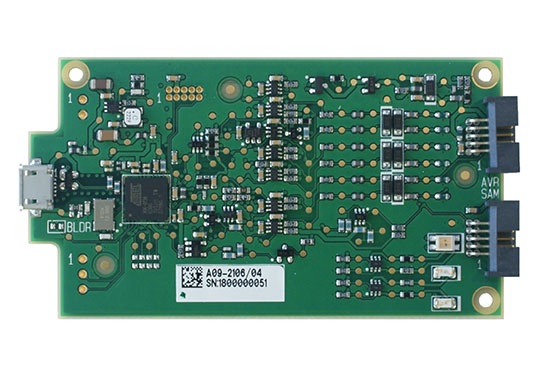
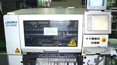
As a professional PCBA manufacturer with more than 20 years of experience in printed circuit board (PCB) soldering and assembly. Grande runs its own PCB factory and SMT factory, which can provide manual soldering, SMT Assembly, and wave soldering processing services.
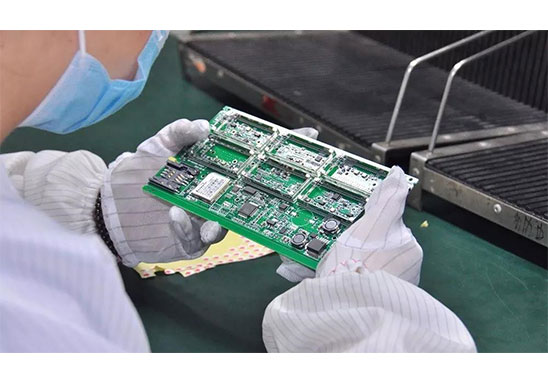
Circuit board soldering ability
1. The largest board: 310mm*410mm (SMT);
2. Maximum board thickness: 3mm;
3. Minimum board thickness: 0.5mm;
4. The smallest Chip component: 0201 package or over 0.6mm*0.3mm;
5. Maximum weight of mounted component: 150 grams;
6. Maximum component height: 25mm;
7. Maximum component size: 150mm*150mm;
8. Minimum lead component spacing: 0.3mm;
9. The smallest spherical component (BGA) spacing: 0.3mm;
10. The smallest spherical component (BGA) diameter: 0.3mm;
11. Maximum component placement accuracy (100QFP): 25um@IPC;
12. Mounting capacity: 3 to 4 million points/day.
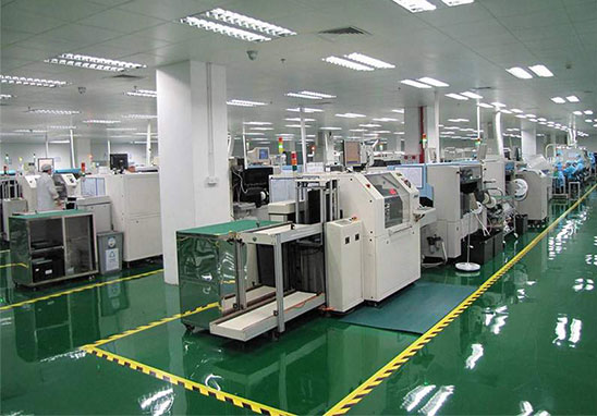
Precautions for circuit board soldering
1. Once got the bare PCB board, you should first conduct an appearance inspection to see if there are short circuits/ open circuits, etc. And then familiarize yourself with the Schematics of the development board, and compare the schematics with the PCB silk screen layer to avoid discrepancies between the schematics and the PCB.
2. After the materials required for circuit board soldering are completed, the components should be classified. Generally speaking, all components can be divided into several categories according to the size, which is convenient for subsequent welding. Need to print a complete list of materials. In the soldering process, if one item is not completed, use a pen to cross out the corresponding option, which is convenient for subsequent soldering operations.
Before soldering, take anti-static measures such as wearing a static ring to avoid damage to the components caused by static electricity. After the equipment required for soldering is ready, the tip of the soldering iron should be kept clean and tidy. BTW, it is recommended to use a flat-angle soldering iron for the first soldering. When soldering components such as 0603 packaged components, the soldering iron can better contact the pads and facilitate soldering. Of course, for sophisticated masters, this is not a problem.
3. When selecting components for soldering, the components should be soldered in the order of low to high and small to large. In order to avoid the soldering of smaller components, the larger components that are soldered will cause inconvenience. Priority is given to soldering integrated circuit chips.
4. Before soldering the integrated circuit chip, ensure that the chip placement direction is correct. For the chip silk screen layer, generally rectangular pads indicate the starting pins. When soldering, fix one pin of the chip first, fine-tune the position of the component, and fix the diagonal pin of the chip, so that the component is accurately connected and then soldered.
6. SMD ceramic capacitors and Zener diodes in voltage regulator circuits have no positive and negative poles. Light-emitting diodes, tantalum capacitors and electrolytic capacitors need to be distinguished between positive and negative poles. For capacitors and diode components, generally the marked end should be negative. In the package of SMD LED, the direction along the lamp is the positive-negative direction. For packaged components marked as diode circuit diagram by silk screen, the negative end of the diode should be placed at the end with a vertical line.
7. For crystal oscillators, passive crystal oscillators generally have only two pins, and there is no difference between positive and negative. Active crystal oscillators generally have four pins. Pay attention to the definition of each pin to avoid soldering errors.
8. For the soldering of plug-in components, such as power module related components, the pins of the device can be modified before soldering. After the components are placed and fixed, the solder is generally melted by a soldering iron on the back and then merged into the front by the pad. There is no need to put too much solder, but the components should be stable first.
9. The PCB design problems found during the soldering process should be recorded in time, such as installation interference, incorrect pad size design, component packaging errors, etc., for subsequent improvements.
10. After soldering, use a magnifying glass to check the solder joints to check whether there are false soldering and short-circuit conditions.
11. After the circuit board soldering is completed, the surface of the circuit board should be cleaned with a cleaning agent such as alcohol to prevent the iron filings attached to the surface of the circuit board from short-circuiting the circuit, and it can also make the circuit board cleaner and more beautiful.
