
What is a via design?
Via is one of the vital components of multilayer PCB, and the cost of drilling usually accounts for 30% to 40% of whole PCB manufacturing cost. From the perspective of PCB design, a via is mainly composed of two parts, one is the drill hole in the middle, and the other is the pad area around the drill. The size of these two parts determines the size of the via size. Obviously, in high-speed and high-density PCB design, designers always hope that the smaller the via hole is, the better, so that more wiring space can be left on the board. In addition, the smaller the via hole, the parasitic capacitance of capacitors its own. The smaller it is, the more suitable it is for high-speed circuits.
However, the reduction in hole size also brings about an increase in cost, and the size of vias cannot be reduced indefinitely. It is limited by process technologies such as drilling and plating: The smaller the via, the longer drilling time the via takes as well as the easier the via is to deviate from the center position; And when the depth of the hole exceeds 6 times the diameter of the drilled via, then it cannot be guaranteed that the via wall can be uniformly plated with copper.
1. In principle, the inner diameter of the all-through hole is >= 0.2mm (8mil), and the outer diameter is >= 0.4mm (16mil) or more. In difficult places, the outer diameter must be controlled to 0.35mm (14mil);
Reminder: According to experience, the inner diameter and outer diameter of PCB commonly used via sizes generally follow X*2±2mil (X represents the inner diameter). For instance, vias with an inner diameter of 8mil can be designed as 8/14mil, 8/16mil or 8/18mil; While vias with 12mil can be designed as 12/22mil, 12/24mil, 12/26mil;
2. It is recommended not to use buried blind vias for BGA designs of 0.65mm and above, as the cost will increase significantly. When using buried blind holes, generally use first-order blind holes (TOP layer-L2 layer or BOTTOM-negative L2). The inner diameter of the via is generally 0.1mm (4mil) and the outer diameter is 0.25mm (10mil), as shown in the figure Shown in 1-1.
Figure 1-1 Schematic diagram of first-order blind hole
3. Vias cannot be placed on pads smaller than the size of the 0402 resistance-capacitance pad; theoretically, the lead inductance is small when placed on the pad, but during production, the solder paste is easy to enter the via, causing uneven solder paste and causing the device to stand up. The phenomenon of getting up (the phenomenon of'stone erecting'). Generally recommended spacing is 4-8mil, as shown in Figure 1-2.
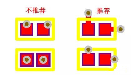
Figure 1-2 Schematic diagram of via hole to pad drilling
4. The spacing between vias and vias should not be too close. Drilling is likely to cause holes. Generally, the hole spacing is required to be 0.5mm and above, 0.35mm-0.4mm should be avoided, and 0.3mm and below are prohibited, as shown in Figure 1-3 Shown.
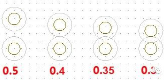
Figure 1-3 The distance between vias and vias
5. As shown in Figure 1-4, except for heat dissipation vias, vias ≤0.5mm need to be plugged with oil (the inner diameter is 0.4mm and need to be plugged).
1) Especially for devices with metal casings, it’s not adviced to drill vias; If drilled, certain plug hole is filled with solder mask to avoid short circuit between the housing and the vias.
2) According to the production feedback of the board factory, it is often mentioned that the vias under the BGA are too close to the pads, and the vias need to be moved. This situation is caused by the fact that the vias are not equidistant from the BGA pads. Because the positions of the vias and test holes under the BAG are not equidistant from the BGA pads, it is a normal state that PCB designers do not pay attention to this. Leading to constant engineering problems, and also a hidden danger to welding quality. Therefore, we directly recommend drilling to the center of the two pads, especially in the BGA due to the small pitch, after drilling, it is necessary to cover the via plugs under the BGA to avoid short circuit of the BGA ball and tin.
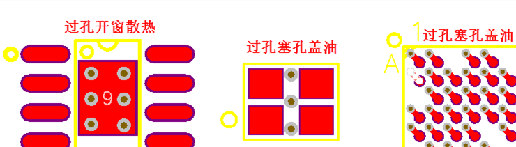
Figure 1-4 Via application scenario
6. The fixed pads of the earphone terminal, buttons, FPC, etc. are used to prevent the copper skin of the pad from falling. If conditions permit, make 1-2 vias on the pad (the vias are evenly placed), which can effectively improve the "fixability" , As shown in Figure 1-5.
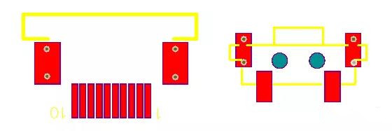
Figure 1-5 The placement of fixed pad vias
7. Fan-shaped hole
Fan-shaped hole is very important in PCB design. The method of fan-shaped hole will affect signal integrity, planar integrity, and the difficulty of wiring, as well as the cost of production.
1) The fan-shaped hole recommendations and defect practices of conventional CHIP devices are shown in Figure 1-6. It can be seen that the recommended practice can be to pass the line between the two holes in the inner layer, and the reference plane will not be split, otherwise it is not recommended to increase In addition to the difficulty of routing, it also splits the reference plane and destroys the integrity of the plane.
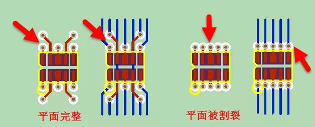
Figure 1-6 Comparison of fan-shaped hole methods of conventional CHIP devices
Similarly, this kind of device sector hole method is suitable for the scenario of punching and changing layers, as shown in Figure 1-7.
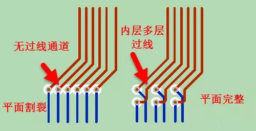
Figure 1-7 Application scenario of hole punching and layer change
2) BGA fan-shaped hole method
BGA fan-shaped holes are also not suitable to be punched on the pads. It is recommended to punch the holes in the middle of the two pads. Many engineers randomly move the position of the via hole in the BGA or even hit the pad for the convenience of the wiring. As shown in Figure 1-8, the irregular via hole in the BGA area can easily cause the problem of late soldering, and it may damage the plane integrity.
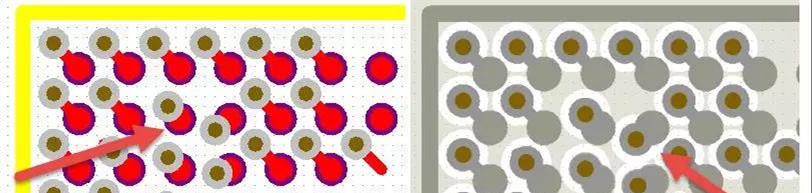
Figure 1-8 Example of the hole in the BGA pads


