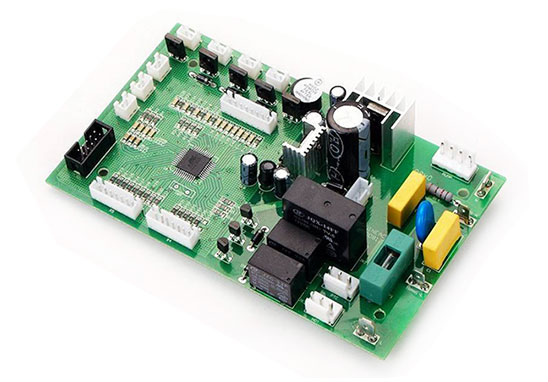
As we all know, a good PCB design engineer should master a wide range of knowledge systems, including electrical theory, component performance, digital and analog circuits, PCBA processing technology and DFM manufacturability theory, welding practice operations, schematic drawing and layout, and single-chip microcomputer programs Logic and basic principles, etc. In other words,
1. If the designed circuit system includes FPGA devices, the Quartus II software must be used to verify the pin assignments before drawing the Schematic. (Some special pins in FPGA cannot be used as ordinary IO).
2. 4-layer board from top to bottom is signal plane layer, ground, power, signal plane layer; While 6-layer board from top to bottom that is signal plane layer, ground, signal inner electric layer, signal inner electric layer, power and signal plane layer. For boards with 6 layers and above (the advantage is: anti-interference radiation), the internal electrical layer wiring is preferred, and the plane layer is not allowed to go. It is forbidden to wire from the ground or power layer ( Mainly considering the power layer will be divided, causing parasitic effects).
3. Routing of multi-power system: If FPGA+DSP system is made of 6-layer board, there will be at least 3.3V+1.2V+1.8V+5V.
3.3V is generally the main power supply, and the power layer is directly laid, and which is easy to route the global power network through the vias;
5V may generally be the power input, and only a small area of copper is required. And as thick as possible.
1.2V and 1.8V are the core power supply (if you directly use the wire connection method, you will encounter great difficulties when facing BGA devices). Try to separate 1.2V and 1.8V during layout, and let 1.2V or 1.8V connect The components are arranged in a compact area and connected by copper
In short, because the power supply network is spread over the entire PCB, it will be very complicated and long to go around if you use the wiring method. At this time, the method of laying copper is a good choice!
4. The routing between adjacent layers adopts a cross method: It is able to reduce electromagnetic interference between parallel wires and facilitate routing.
5. What is the isolation method for analog and digital isolation? Separate the devices used for analog signals and digital signals during layout, and then cut across the AD chip!
The analog signal is laid with an analog ground, and the analog ground/analog power supply and the digital power supply are connected at a single point through an inductor/magnetic bead.
6. PCB design based on PCB design software can also be regarded as a software development process. Software engineering pays most attention to the idea of "iterative development" to reduce the probability of PCB errors.
(1) Check the schematic diagram, pay special attention to the power and ground of the device (power and ground are the blood of the system, and there can be no negligence);
(2) PCB package drawing (confirm whether the pins in the schematic diagram are wrong);
(3) After confirming the PCB package size one by one, add a verification label and add it to the package library of this design;
(4) Import the netlist and adjust the signal sequence in the schematic while layout (OrCAD component automatic numbering function can no longer be used after layout).
In the specific PCB design process, the basic knowledge that need to be mastered includes:
1. Preliminary Preparation
Including the preparation of component libraries and Schematic. Before proceeding with PCB design, we must first prepare the schematic SCH component library and PCB component packaging library.
The PCB component package library is best established by the engineer based on the standard size data of the selected device. In principle, establish the PC component package library first, and then establish the schematic SCH component library.
PCB component packaging library requirements are high, it directly affects the installation of PCB; schematic SCH component library requirements are relatively loose, but pay attention to define the pin attributes and the corresponding relationship with the PCB component packaging library.
2. PCB Structure Design
According to the determined circuit board size and various mechanical positioning, draw the PCB frame in the PCB design environment, and place the required connectors, buttons/switches, screw holes, assembly holes, etc. according to the positioning requirements.
Fully consider and determine the wiring area and non-wiring area (such as how much area around the screw hole belongs to the non-wiring area).
3. PCB Layout
PCB Layout is to place the devices in the PCB frame according to the design requirements. Generate the netlist (Design→CreateNetlist) in the schematic tool, and then import the netlist (Design→ImportNetlist) in the PCB software. After the netlist is successfully imported, it will exist in the background of the software. Through the Placement operation, all devices can be called out, and there is a flying line prompt connection between the pins. At this time, the layout design of the device can be carried out.
PCB layout is the first important process in the entire PCB design process. The more complex the PCB board, the better the layout can directly affect the difficulty of later wiring.
The layout design relies on the circuit board designer's basic circuit knowledge and rich design experience, which is a higher level requirement for the circuit board designer. The junior circuit board designer has little experience and is suitable for small module layout design or PCB layout tasks with lower difficulty of the whole board.
4. PCB Routing
PCB routing is the process with the largest workload in the whole PCB design, which directly affects the performance of PCB board.
In the PCB design process, there are three various levels about PCB routing:
>Routing reasonably, which is the most basic entry requirement for PCB design;
>The satisfaction of electrical performance, which is a standard to measure whether a PCB board is qualified. After the Layout is initially finished, carefully adjust the routing to achieve the best electrical performance;
>Neat and beautiful PCB Layout. Messy routing, even if the electrical performance is passed, it will still bring extremely inconvenience to the optimization of the later board modification, testing and maintenance. Therefore, for PCB Layout, routing always require neat and uniform instead of criss-cross and disorderly.
5. Routing Optimization & Silk Screen Placement
"PCB design never be the best, only better", "PCB design is an art of defects", this is mainly because PCB design need to realize the design requirements of all aspects of hardware, and individual requirements may be in conflict.
For instance, a PCB design project need to be designed as a 6-layer board after evaluation by the circuit board designer; However, the product hardware must be designed as a 4-layer board due to cost considerations, so the signal shielding ground layer can only be sacrificed, resulting in adjacent routing whose signal crosstalk between layers increases but signal quality decreases.
The general design experience is: Time in optimizing routing is twice of the first routing. After the PCB layout optimization is completed, post-processing is required. The first thing to do is the silk screen logo on the PCB surface. Also, the bottom silk screen letters need to be mirrored during design to avoid confusion with the top silk screen.
6. Network DRC Inspection & Structure Inspection
Quality control is an important part during PCB design process. General quality control methods include: Self-inspection, mutual inspection, expert review meetings, special inspections, etc.
Schematic and structural element diagrams are the most basic design requirements. Network DRC inspection and structural inspection are to confirm that the PCB design meets the two input conditions of the schematic netlist and structural element diagram.
Generally, circuit board designers will have their own accumulated design quality inspection checklist, in which some items come from the company or department's specifications, and the other part comes from their own experience summaries. Special inspections include Valor inspection and DFM inspection of the design. These two parts focus on the PCB design output back-end processing gerber file.
7. PCB Manufacturing
Before PCB is formally manufactured, the circuit board designer need to communicate with the PE of the PCB supplier and answer the manufacturer's confirmation questions about PCB manufacturing. (EQ Confirmation Stage, EQ-Engineer Questions)
It includes but not limited: Choice of PCB board model, adjustment of circuit layer line width and line spacing, adjustment of impedance control, adjustment of PCB stacking thickness, surface treatment processing technology, aperture tolerance control and delivery standards, etc.