The processing of the power plane occupies a very important position in PCB layout. In a completed design project, the processing of the power supply can usually determine the success rate of this project by 30%-50%. Now Grande will introduce the basic elements about power plane that should be considered in PCB layout.
1. When handling power, the first thing should be considered that is its current carrying capacity, which contains two aspects:
(a) Whether the power line width or copper sheet width is sufficient or not. To consider the power line width, we must first understand the copper thickness of the layer where the power signal is processed. The copper thickness of the PCB outer layer (TOP/BOTTOM layer) under the conventional process is 1oz (35um), and the inner copper thickness will be based on the actual situation. 1oz or 0.5oz. For 1oz copper thickness, under normal circumstances, 20mil can carry about 1A current; 0.5oz copper thickness, under normal circumstances, 40mil can carry about 1A current.
(b) Whether the size and number of vias meet the power supply current capacity when changing layers. First of all, we must understand the flow capacity of a single via. Under normal circumstances, the temperature rise is 10 degrees. You can refer to the following table.
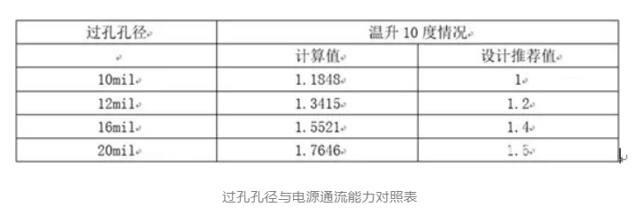
As can be seen from the above table, a single 10mil via can carry 1A of current, so when designing, if the power supply is 2A, then using 10mil vias to punch and change layers, at least 2 vias must be punched. Generally, when designing, you will consider drilling a few more holes in the power channel to maintain a little margin.
2. Secondly, the power supply path should be considered. Specifically, the following 4 aspects should be considered:
(a) The power path should be as short as possible. If it goes too long, the voltage drop of the power supply will be more serious, and the voltage drop will cause the project to fail.
(b) The division of the power plane should be as regular as possible, and slender and dumbbell-shaped divisions are not allowed.
(c) When dividing the power supply, try to keep the separation distance between the power supply and the power plane at about 20 mils. If the BGA is a part of the area, the separation distance of 10 mils can be locally maintained. If the power plane and the plane are too close, there may be a risk of short circuit.
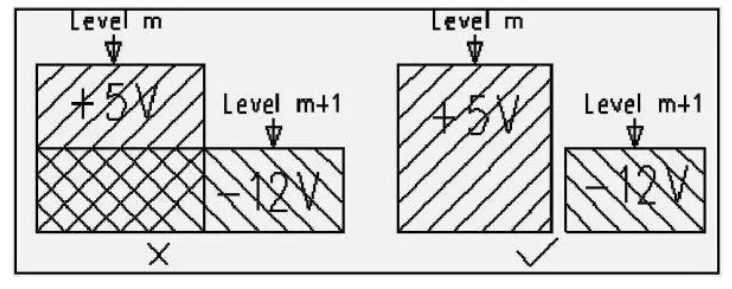
(d) If handling power supplies on adjacent planes, try to avoid parallel handling of copper sheets or traces. The main purpose is to reduce the interference between different power supplies, especially between power supplies with very different voltages. The problem of power plane overlap must be avoided. If it is unavoidable, consider the intermediate ground.
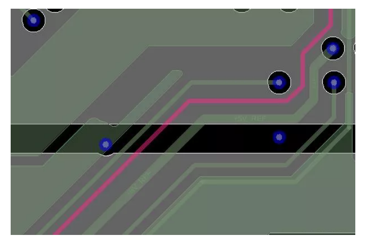
At the time of dividing the power supply, try to avoid the cross-segmentation of adjacent signal lines. If the signal is cross-segmented (the red signal line has a cross-segment phenomenon as shown below), there will be impedance mutations due to the discontinuity of the reference plane, which will cause EMI and crosstalk problems. While doing high-speed PCB layout, cross-segmentation will greatly affect the signal quality.